The world-class technologies and expertise at our core facilities and research centers support a unified, multidisciplinary research & innovation ecosystem across Cornell’s rural and urban campuses.
Research Services supports researchers and research administrators through every step of the research endeavor, from preparing a proposal and developing corporate partnerships to managing a project and ensuring compliance.
Cornell’s technology translation offices and programs work with researchers, investors, and industry partners to bring Cornell inventions from the lab to the marketplace.
Research and Innovation at Cornell
Unparalleled Quality and Breadth
Cornell researchers are leaders in their fields, with specialized expertise and diverse approaches to understanding our world and solving problems.
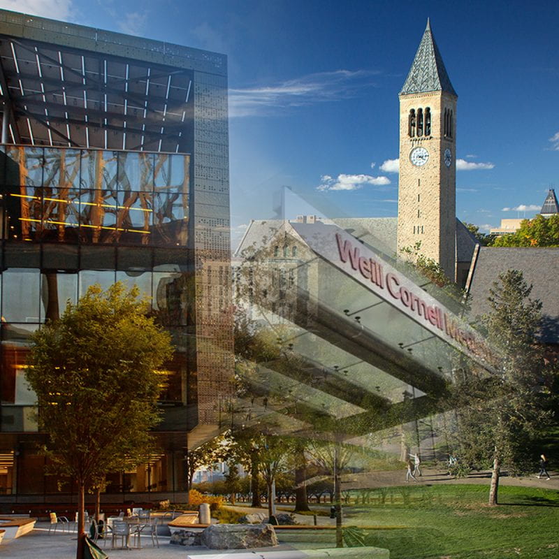
Colleges and Schools at the Ithaca Campus →
Weill Cornell Medicine →
Cornell AgriTech →
Cornell Tech →
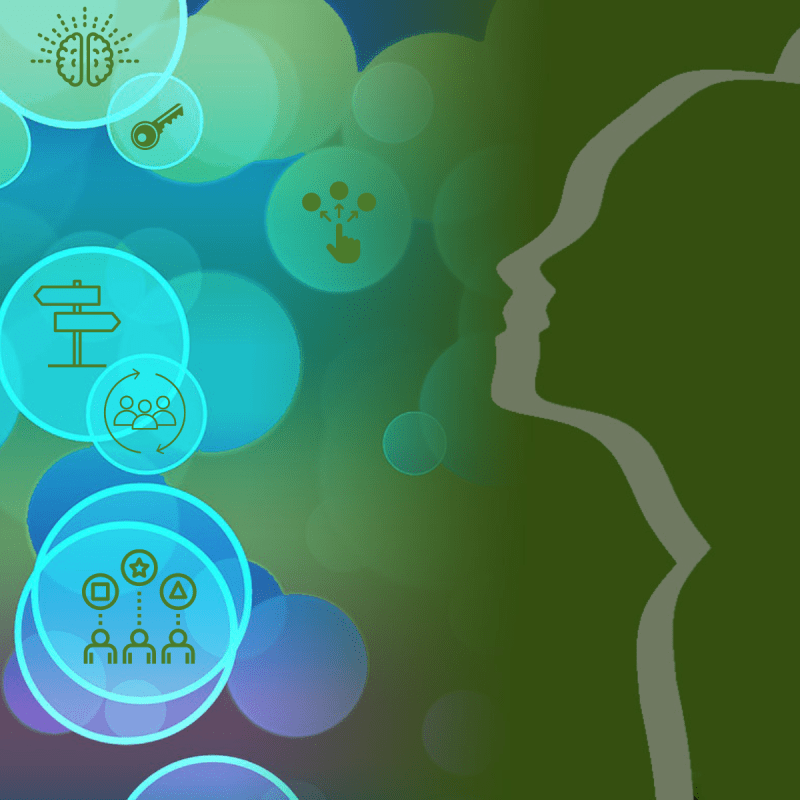
Culture of Collaboration
With world-class research facilities and unparalleled quality and breadth of expertise, Cornell fosters a rich environment for collaborations. The complementary resources of Cornell’s rural and urban campuses create unique opportunities to pursue holistic, transdisciplinary approaches to complex challenges.
Academic Integration →
Provost’s Radical Collaboration Initiative →


Vibrant Innovation Ecosystem
A network of specialized business incubators, seed funding opportunities, competitions, mentorship programs, and other resources give researchers and entrepreneurs the training and support they need to translate ideas and discoveries into innovations that benefit people and communities around the world.
Innovation and Entrepreneurship Overview →
Center for Life Sciences Ventures →
Center for Regional Economic Advancement (CREA) →
Praxis Center for Venture Development →
Entrepreneurship at Cornell →
Commitment to Diversity and Inclusion
Our goal is for faculty, students, and staff to bring the diversity of backgrounds and experiences necessary for radical collaborations and impactful research. To be successful we must have a culture of inclusion, equity, collaboration, and change. We affirm the institutional initiatives led by the Office of the President.
Belonging at Cornell →
Institutional Initiatives →
Diversity & Inclusion Resources →

Enhancing Lives
Cornell is committed to the transfer of knowledge and discoveries, the commercialization of new technology, sustainable economic development, and job creation, which work together to improve the quality of life for people and communities spanning the globe.
Public Engagement →
Cornell Cooperative Extension →
Bronfenbrenner Center for Translational Research →